Chemical Mechanical Planarisation
Polishing very thin films of diamond is problematic, as the curvature of the substrate (the wafer bow) can be much greater than the thickness of the film. This is exaggerated in the below left image, but generally 2” silicon wafers can have a bow exceeding several microns. Obviously, attempting to conventionally polish a 300 nm thick diamond film on a flat schaife would be catastrophic as the middle of the wafer would be polished through to the silicon before the edges of the wafer are even touched. Conventional scaife polishing is also far too aggressive for 500 µm thick silicon wafers, tending to shatter them on contact. Lapping / scaife polishing also creates sub surface damage which limits the coherence time of NV/SiV centres in diamond for quantum technologies, reduces carrier lifetimes / charge collection efficiency in detectors and increases dissipation in Surface Acoustic Wave devices.

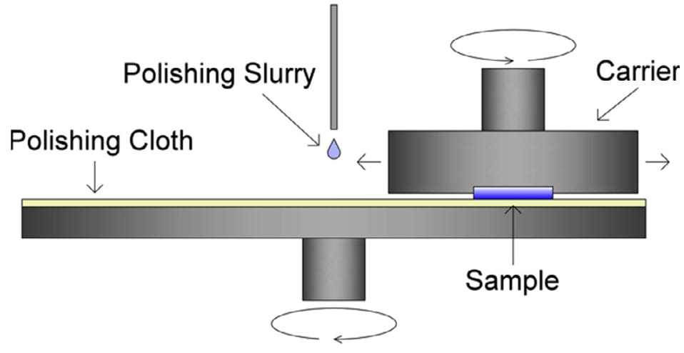
The solution we have found is to use a polishing approach that compensates for the wafer bow, and to this end we adapt conventional Chemo - Mechanical Polishing (CMP) techniques as used in the silicon industry to diamond (see above right). In this process a polishing slurry (in this case Syton SF1) is applied to a polishing pad (Suba - X). The pad is not as hard as a conventional schaife, and thus the wafer sinks into it, compensating for the bow. The wafer carrier can also compensate for bow by applying a backing pressure. The polishing cloth and wafer carrier are rotated in opposite directions at 60 rpm and the down pressure is around 4 psi, at least an order of magnitude less than conventional schaife polishing. Several examples of different diamond materials before and after polishing are show below.
Nanocrystalline diamond CMP
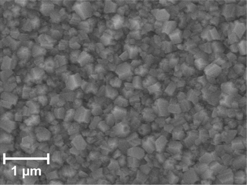
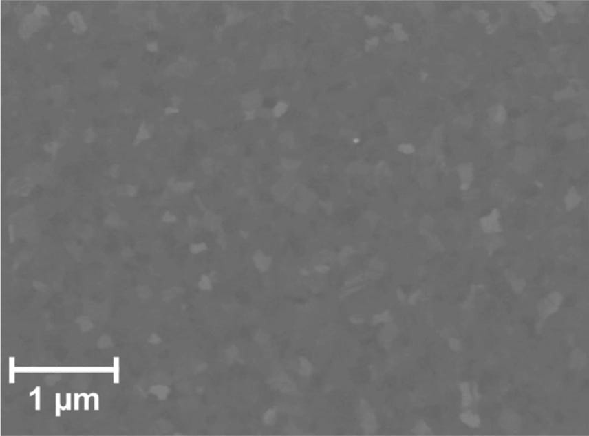
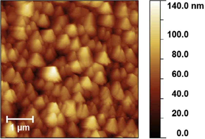
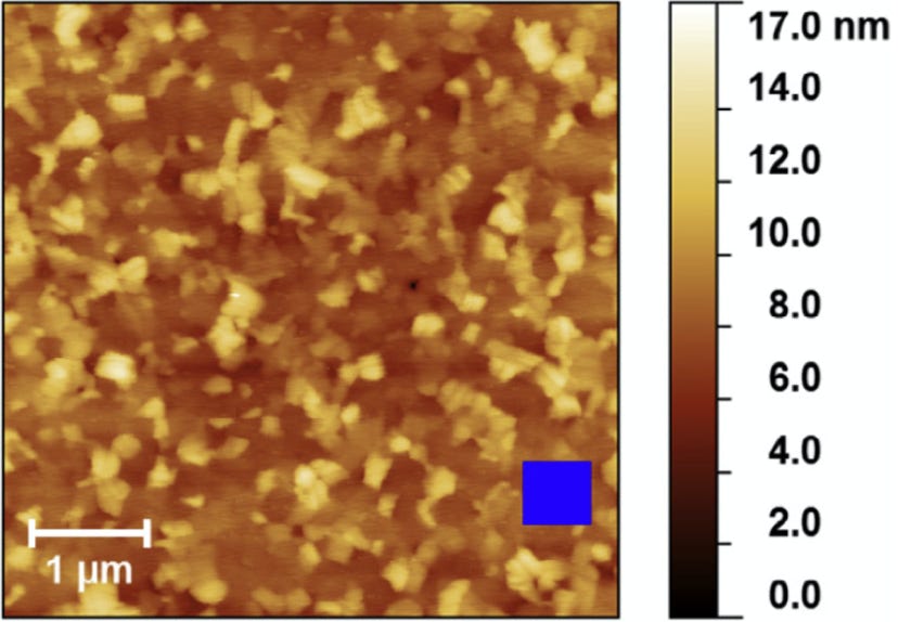
The electron micrographs above show 350 nm thick nanocrystalline diamond films before and after 4 hours of CMP. It is clear that before CMP, the films have a typical polycrystalline morphology of grains in the order of a few hundred nm. After 4 hours of CMP this texture is barely visible and the films exhibit very little texture in electron microscopy. Atomic Force Microscopy (AFM, see below) shows that the rms roughness of the 350 nm thick films can be reduced to below 2 nm rms over 25 µm2, and less than 0.5 nm rms in localised areas (blue square).
See Thomas et al, Carbon 68 (2014) 473
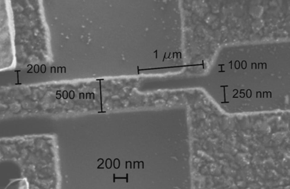
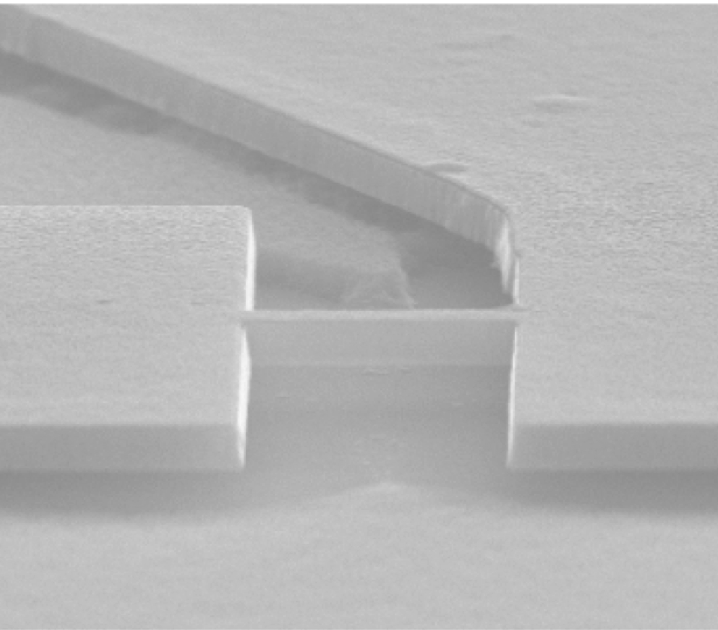
A critical application of CMP is reducing the surface roughness of nanocrystalline diamond (NCD) so that nanodevices can easily be fabricated from it. The surface roughness of NCD is ofter some 10’s of nm rms, which is comparable to the feature size of some of the devices we fabricate. In the electron microscopy images below, the left image is a microelectromechanical device fabricated in collaboration with Boston University (see Imboden et al, NL 13 (2013) 4014) before we had developed CMP. You can clearly see the granularity of the material, the grain size being about the same as the smallest feature. This dramatically reduces yield. The bottom right image shows devices fabricated after CMP, here no granularity is observable and the material behaves similar to silicon technology.
Single Crystal Diamond
All conventional polishing and lapping techniques introduce very fine scratches in diamond. These are shown below left in an Atomic Force Microscopy (AFM) of a {111} oriented single crystal diamond. The parallel line crossing the sample are nano grooves resulting from the original polish. We are able to remove these nano grooves using CMP, this is visible bottom right. Another advantage of CMP is that it is not sensitive to different directions on {111} or {100} surface like conventional approaches and doesn’t create ay sub surface damage.
See Thomas et al, STAM 15 (2014) 035013


More information
We continue to research CMP of diamond and other materials, for more information see our publications:
Thomas et al, Carbon 68 (2014) 473 (NCD, first diamond CMP using colloidal silica)
Thomas et al, STAM 15 (2014) 035013 (Single Crystal {100} and {111} diamond)
Werrell et al, STAM 18 (2017) 654 (other slurries such as alumina and ceria)
Mandal et al, Carbon 130 (2018) 25 (rate enhancement by redox agent addition)